Tutorial Start by tapping on Next button.
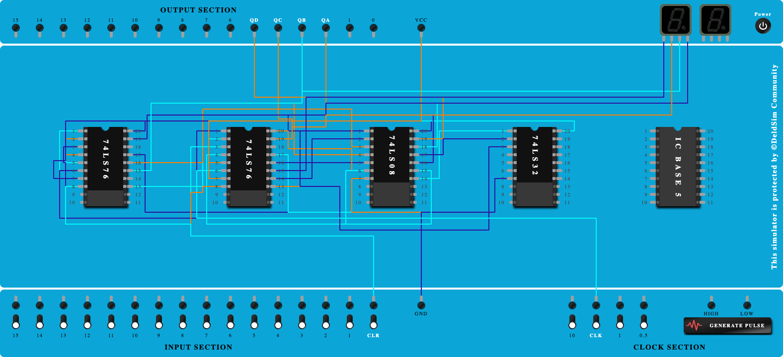
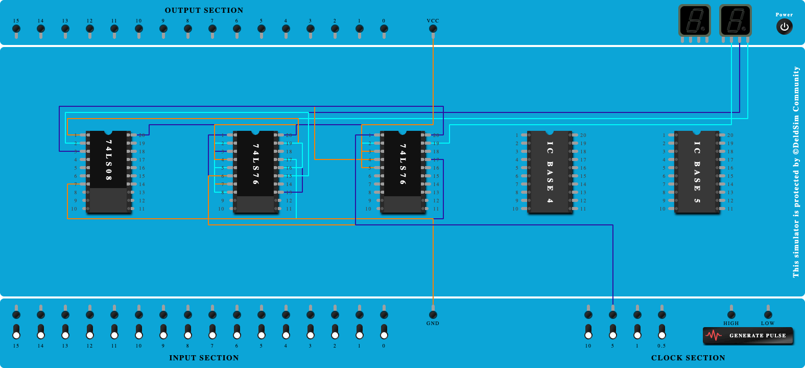
1. Click on 'Next' button to Add IC-74LS76, 74LS08, 74LS32 Click on 'Next' button to Add IC-74LS76, 74LS08, 74LS32
2. Click on 'Next' button to Connect GND and VCC of ICs Click on 'Next' button to Connect GND and VCC of ICs
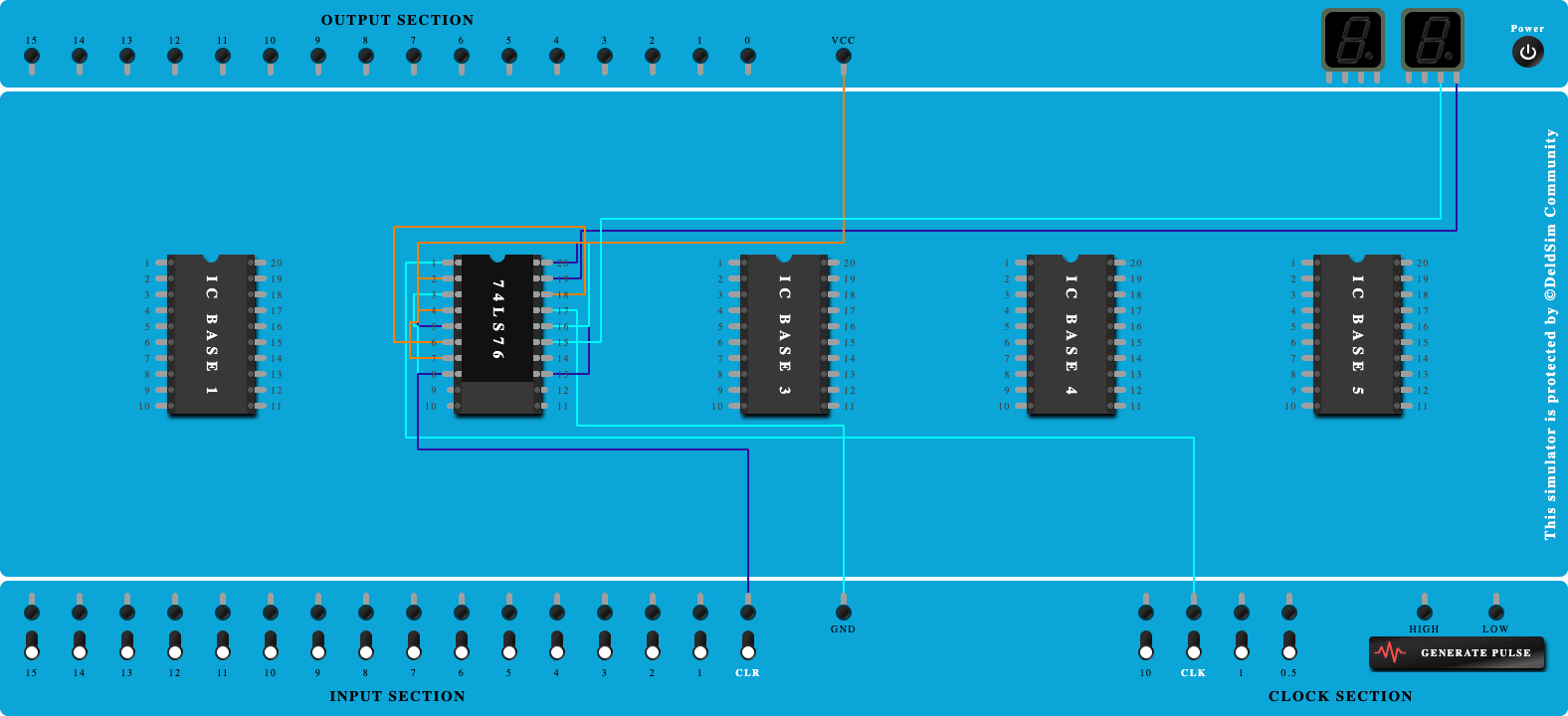
3. Click on 'Next' button to Connect J1, K1 to Vcc Click on 'Next' button to Connect J1, K1 to Vcc
4. Click on 'Next' button to Connect Clock Pin-1 to clock port Click on 'Next' button to Connect Clock Pin-1 to clock port
5. Click on 'Next' button to Connect QA to Output port Click on 'Next' button to Connect QA to Output port
6. Click on 'Next' button to Connect QA to Pin-1 of AND Gate Click on 'Next' button to Connect QA to Pin-1 of AND Gate
7. Click on 'Next' button to Connect output of AND Gate to J2,K2 Click on 'Next' button to Connect output of AND Gate to J2,K2
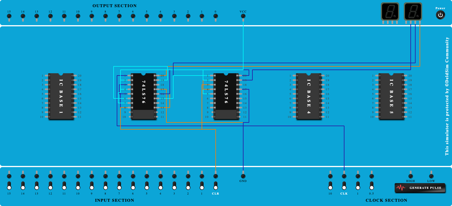
8. Click on 'Next' button to Connect Clock Pin-2 to clock port Click on 'Next' button to Connect Clock Pin-2 to clock port
9. Click on 'Next' button to Connect QB to output port Click on 'Next' button to Connect QB to output port
10. Click on 'Next' button to Connect QB to Pin-4 of AND Gate Click on 'Next' button to Connect QB to Pin-4 of AND Gate
11. Click on 'Next' button to Connect QA to Pin-5 of AND Gate Click on 'Next' button to Connect QA to Pin-5 of AND Gate
12. Click on 'Next' button to Connect Output-2 of AND Gate to J3,K3 Click on 'Next' button to Connect Output-2 of AND Gate to J3,K3
13. Click on 'Next' button to Connect Clock Pin-3 to clock port Click on 'Next' button to Connect Clock Pin-3 to clock port
14. Click on 'Next' button to Connect Output-2 of AND Gate to Pin-9 of AND Gate Click on 'Next' button to Connect Output-2 of AND Gate to Pin-9 of AND Gate
15. Click on 'Next' button to Connect QC to output port Click on 'Next' button to Connect QC to output port
16. Click on 'Next' button to Connect QC to pin-10 of AND Gate Click on 'Next' button to Connect QC to pin-10 of AND Gate
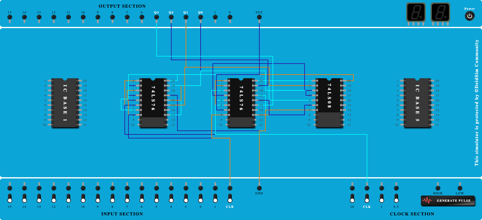
17. Click on 'Next' button to Connect Output-3 of AND Gate to input-1 of OR Gate Click on 'Next' button to Connect Output-3 of AND Gate to input-1 of OR Gate
18. Click on 'Next' button to Connect Output of OR Gate to J4,K4 Click on 'Next' button to Connect Output of OR Gate to J4,K4
19. Click on 'Next' button to Connect Clock Pin-4 to clock port Click on 'Next' button to Connect Clock Pin-4 to clock port
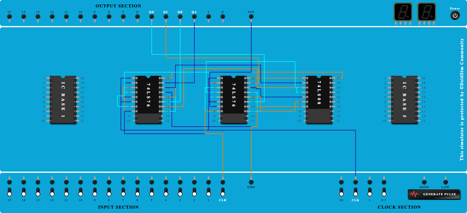
20. Click on 'Next' button to Connect QD to output port Click on 'Next' button to Connect QD to output port
21. Click on 'Next' button to Connect -QD to pin-2 of AND Gate Click on 'Next' button to Connect -QD to pin-2 of AND Gate
22. Click on 'Next' button to Connect QA to pin-18 of AND Gate Click on 'Next' button to Connect QA to pin-18 of AND Gate
23. Click on 'Next' button to Connect QD to pin-19 of AND Gate Click on 'Next' button to Connect QD to pin-19 of AND Gate
24. Click on 'Next' button to Connect pin-17 of AND Gate to pin-2 of OR Gate Click on 'Next' button to Connect pin-17 of AND Gate to pin-2 of OR Gate
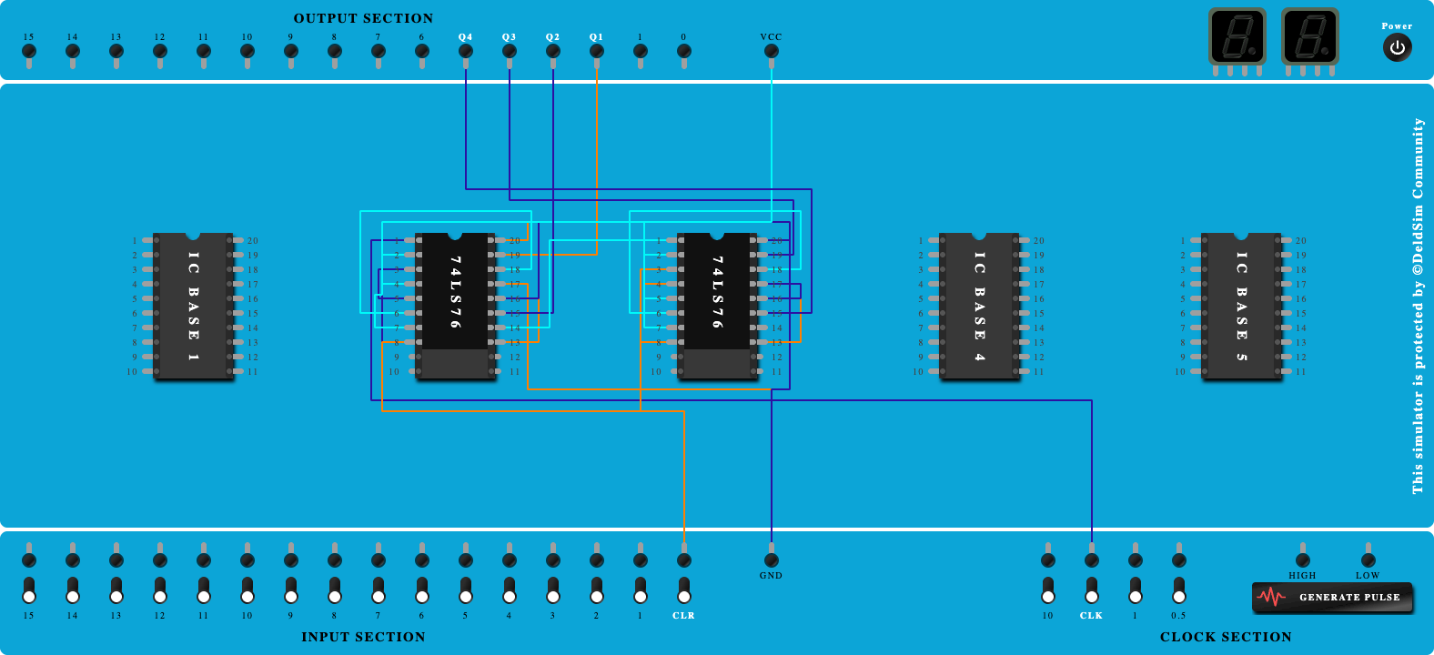
25. Click on 'Next' button to Connect CLEAR Pins of all ICs to Input port Click on 'Next' button to Connect CLEAR Pins of all ICs to Input port
26. Click on 'Next' button to Connect PR Pins of all ICs to Vcc port Click on 'Next' button to Connect PR Pins of all ICs to Vcc port
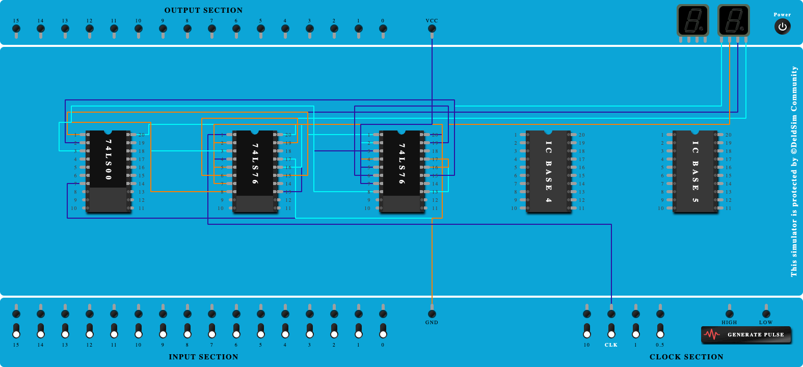
27. Click on 'Next' button to Connect Outputs to 7-seg display to better understanding of counter (Optional) Click on 'Next' button to Connect Outputs to 7-seg display to better understanding of counter (Optional)
Done You have completed the tutorial. Power on the circuit to test the behavior.