Tutorial Start by tapping on Next button.
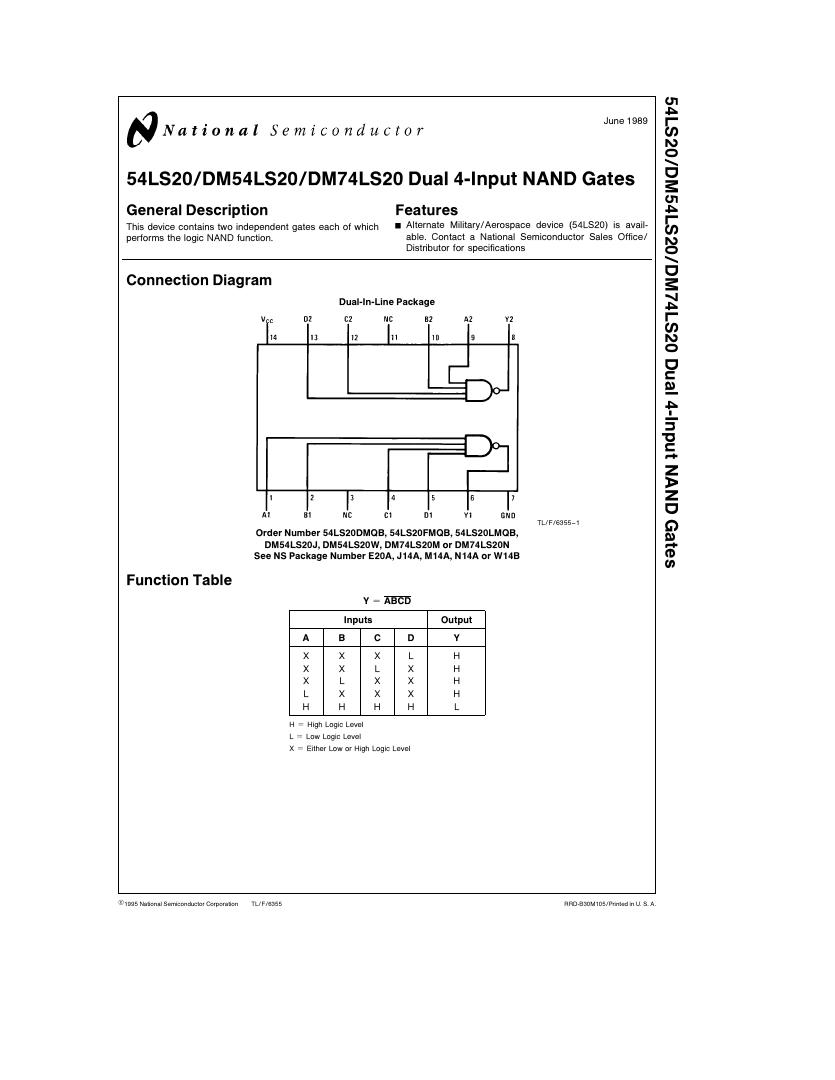
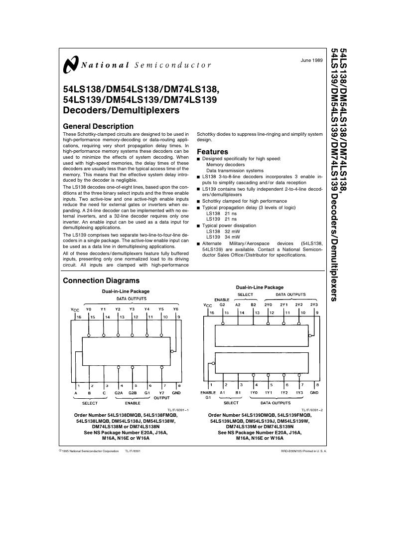
1. Click on 'Next' button to Add 74LS20 and 74LS138 IC Click on 'Next' button to Add 74LS20 and 74LS138 IC
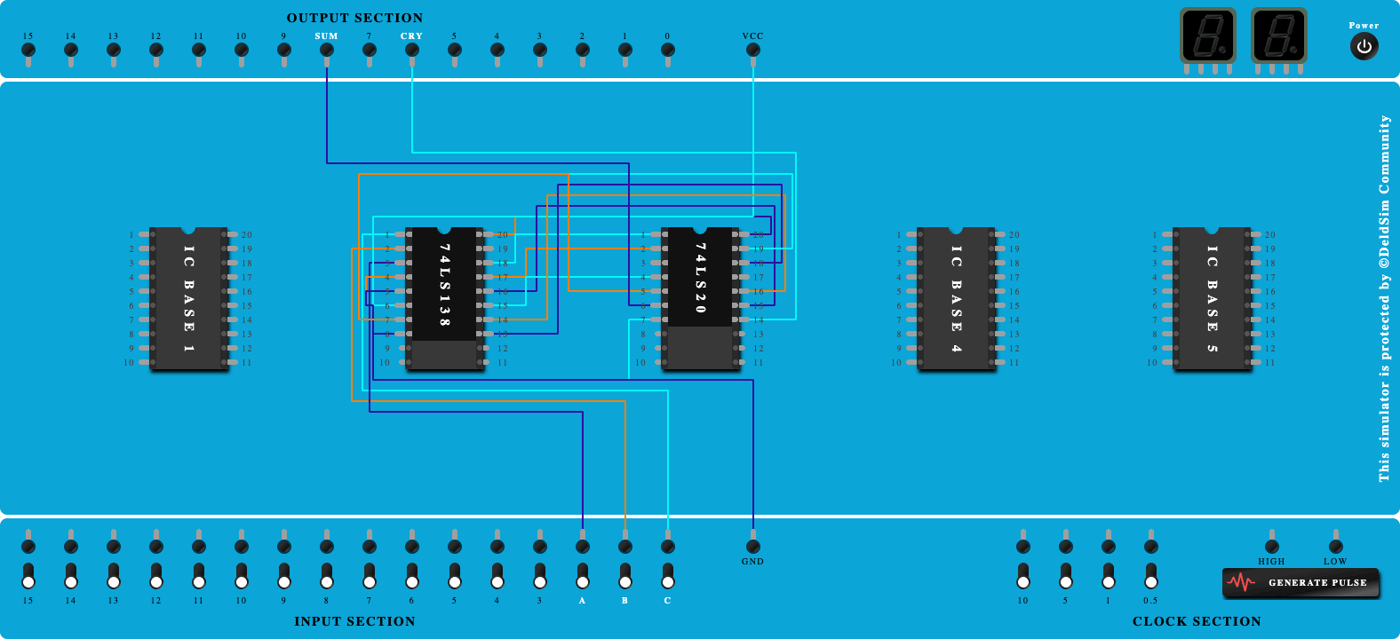
2. Click on 'Next' button to Connect GND and VCC of ICs Click on 'Next' button to Connect GND and VCC of ICs
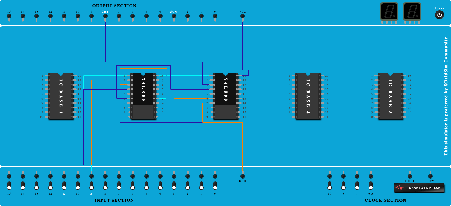
3. Click on 'Next' button to Connect select line 'C' to Pin-1 of IC Click on 'Next' button to Connect select line 'C' to Pin-1 of IC
4. Click on 'Next' button to Connect select line 'B' to Pin-2 of IC Click on 'Next' button to Connect select line 'B' to Pin-2 of IC
5. Click on 'Next' button to Connect select line 'A' to Pin-3 of IC Click on 'Next' button to Connect select line 'A' to Pin-3 of IC
6. Click on 'Next' button to Connect 'G1' to Vcc Click on 'Next' button to Connect 'G1' to Vcc
7. Click on 'Next' button to Connect 'G2A' to GND Click on 'Next' button to Connect 'G2A' to GND
8. Click on 'Next' button to Connect 'G2B' to GND Click on 'Next' button to Connect 'G2B' to GND
9. Click on 'Next' button to Connect Output 'Y1' to Pin-1 of NAND Gate-1 Click on 'Next' button to Connect Output 'Y1' to Pin-1 of NAND Gate-1
10. Click on 'Next' button to Connect Output 'Y2' to Pin-2 of NAND Gate-1 Click on 'Next' button to Connect Output 'Y2' to Pin-2 of NAND Gate-1
11. Click on 'Next' button to Connect Output 'Y3' to Pin-9 of NAND Gate-2 Click on 'Next' button to Connect Output 'Y3' to Pin-9 of NAND Gate-2
12. Click on 'Next' button to Connect Output 'Y4' to Pin-4 of NAND Gate-1 Click on 'Next' button to Connect Output 'Y4' to Pin-4 of NAND Gate-1
13. Click on 'Next' button to Connect Output 'Y5' to Pin-16 of NAND Gate-2 Click on 'Next' button to Connect Output 'Y5' to Pin-16 of NAND Gate-2
14. Click on 'Next' button to Connect Output 'Y6' to Pin-12 of NAND Gate-2 Click on 'Next' button to Connect Output 'Y6' to Pin-12 of NAND Gate-2
15. Click on 'Next' button to Connect Output 'Y7' to Pin-13 of NAND Gate-2 Click on 'Next' button to Connect Output 'Y7' to Pin-13 of NAND Gate-2
16. Click on 'Next' button to Connect Output 'Y7' to Pin-5 of NAND Gate-1 Click on 'Next' button to Connect Output 'Y7' to Pin-5 of NAND Gate-1
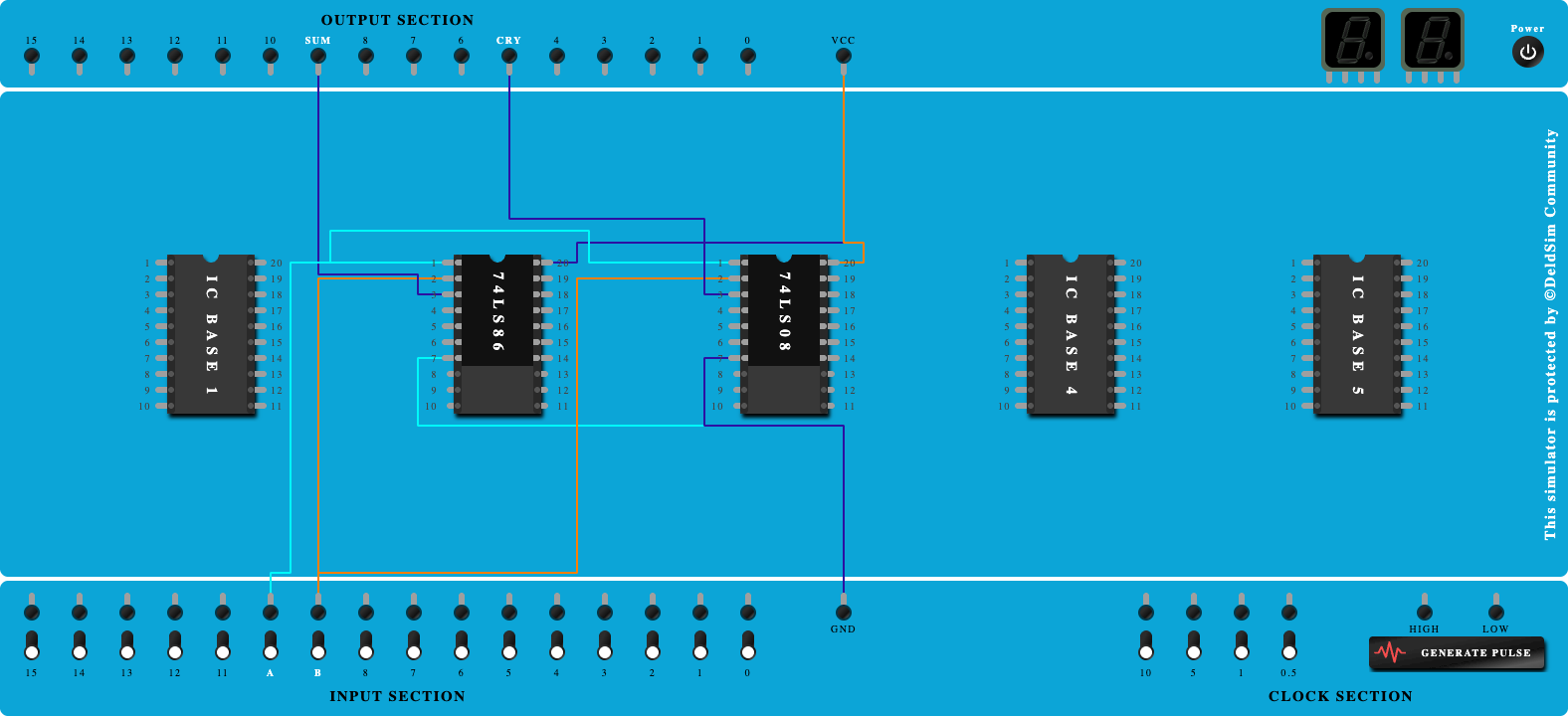
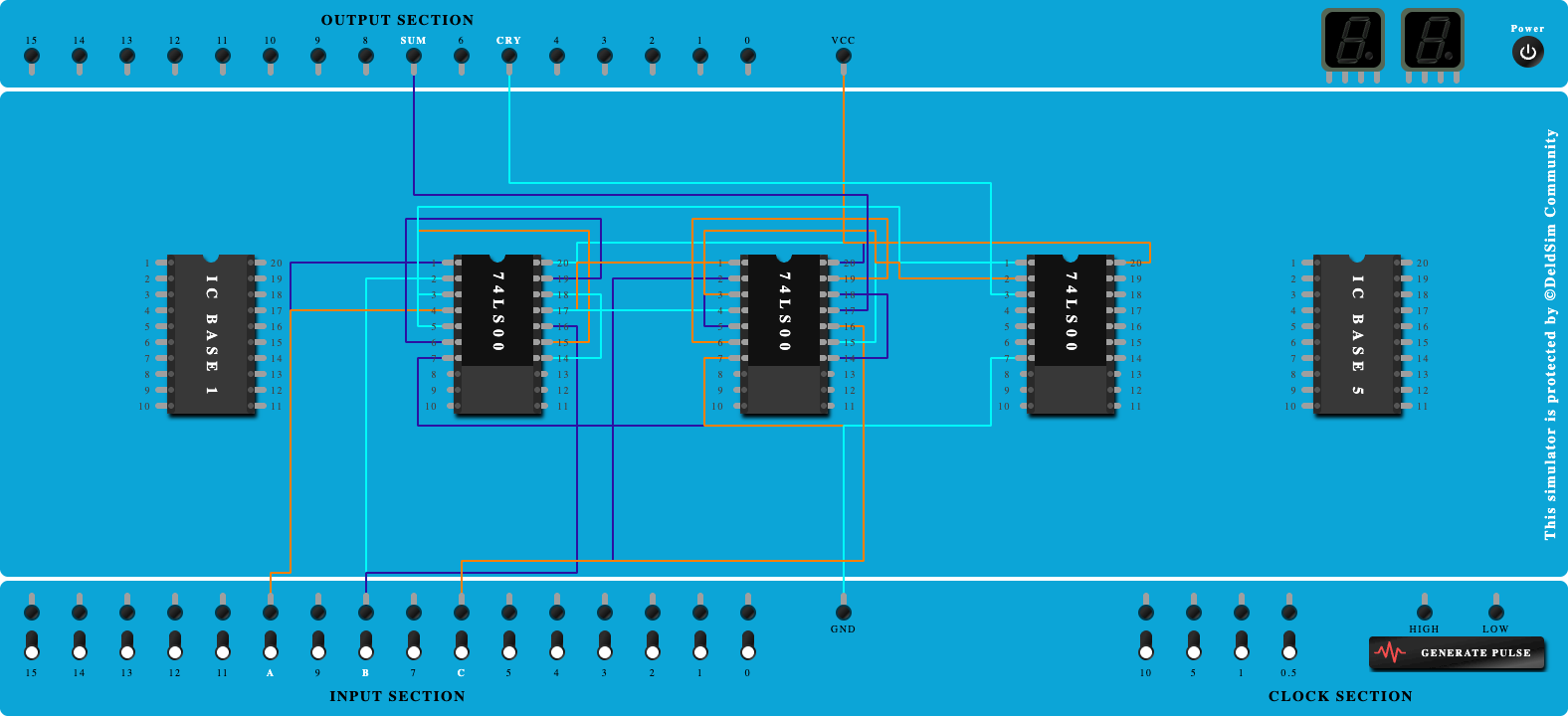
17. Click on 'Next' button to Connect Output of NAND Gate-1 to Output Port as 'SUM' Click on 'Next' button to Connect Output of NAND Gate-1 to Output Port as 'SUM'
18. Click on 'Next' button to Connect Output of NAND Gate-2 to Output Port as 'CARRY' Click on 'Next' button to Connect Output of NAND Gate-2 to Output Port as 'CARRY'
Done You have completed the tutorial. Power on the circuit to test the behavior.