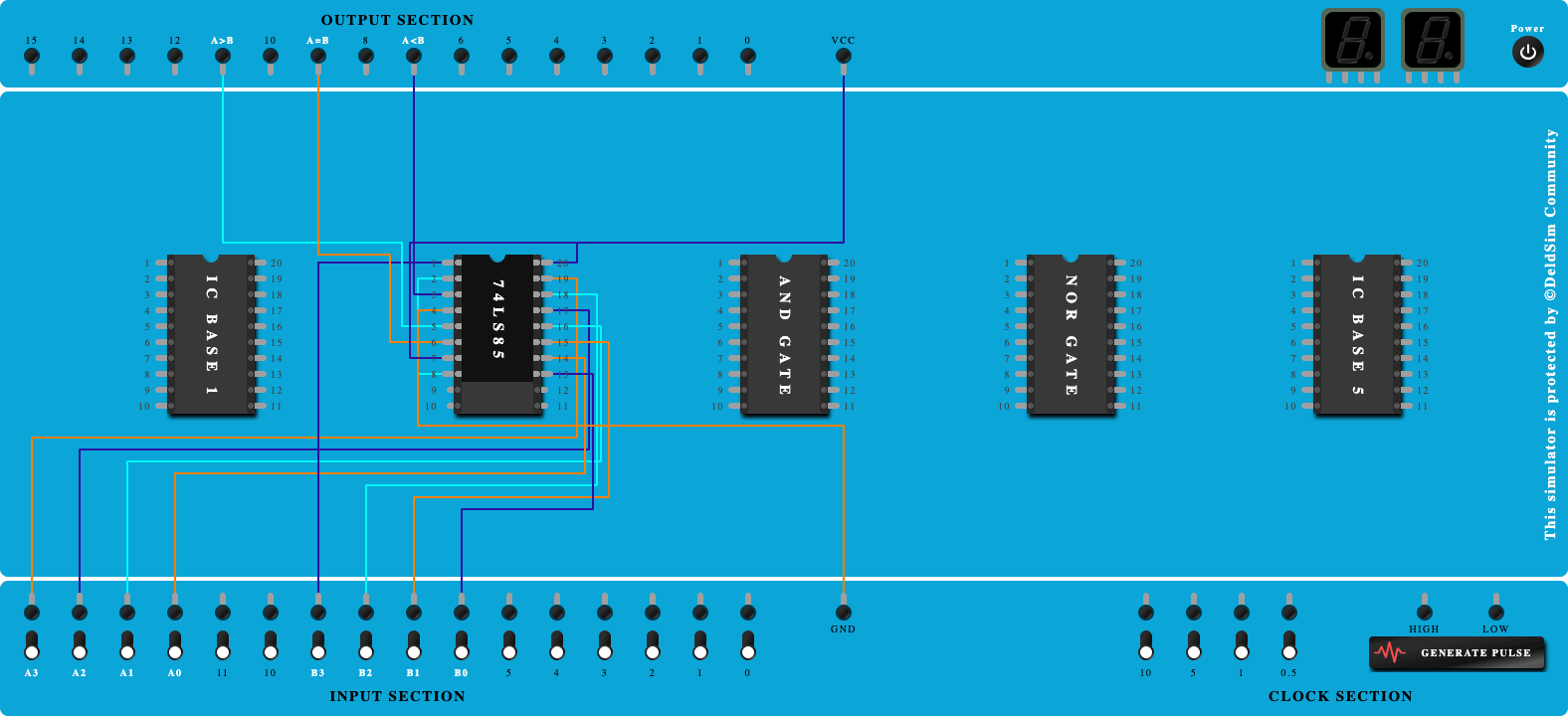
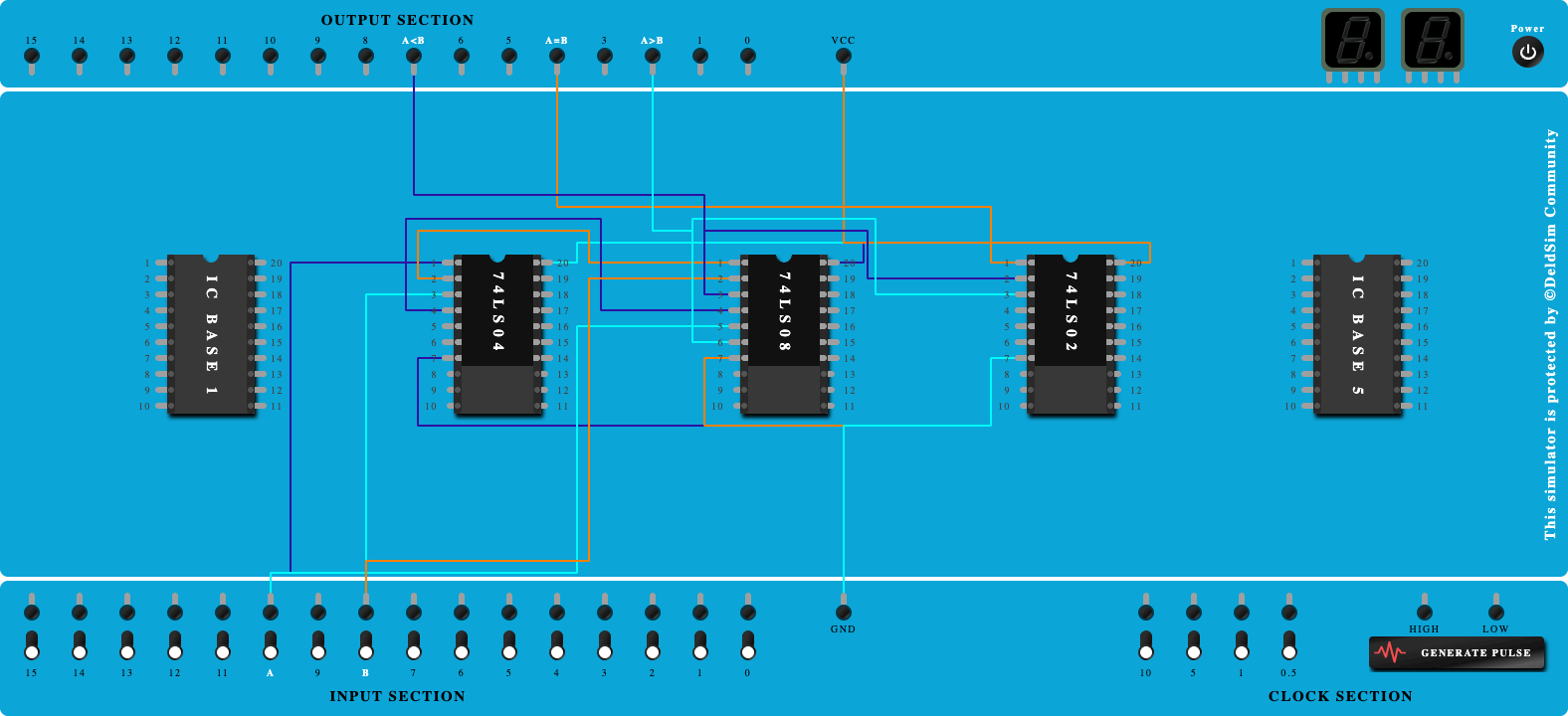
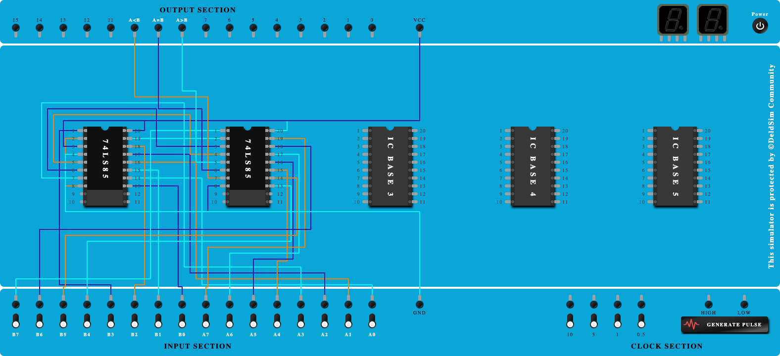
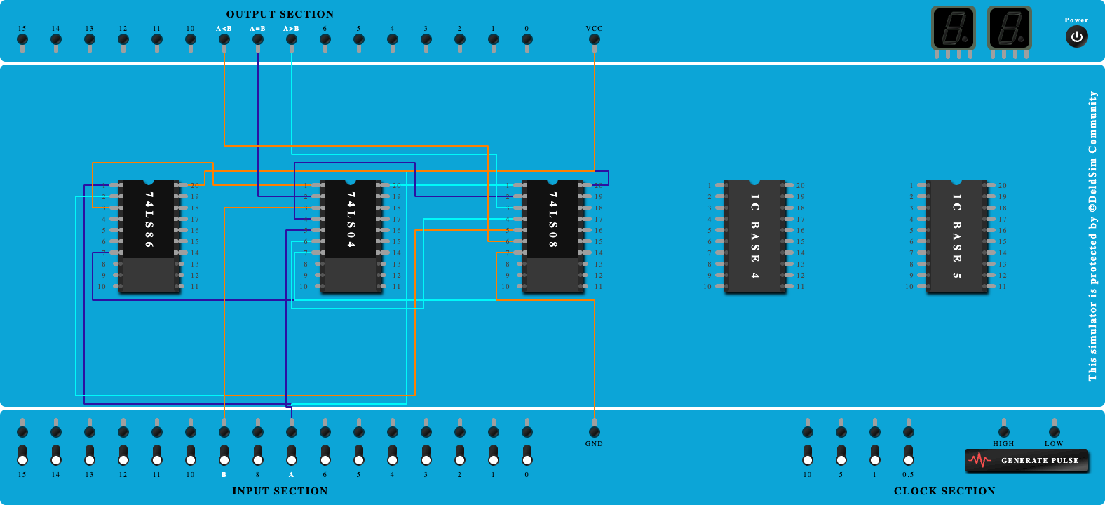
One Bit Comparator

100%
Step-by-Step Procedure
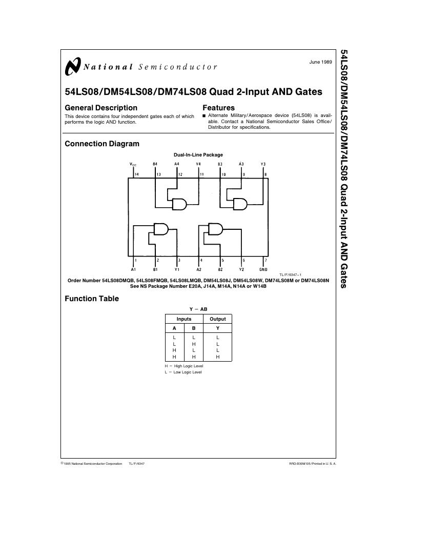
- Click on 'Next' button to Add ICs-74LS86, 74LS04 and 74LS08
- Click on 'Next' button to Connect GND and VCC of ICs
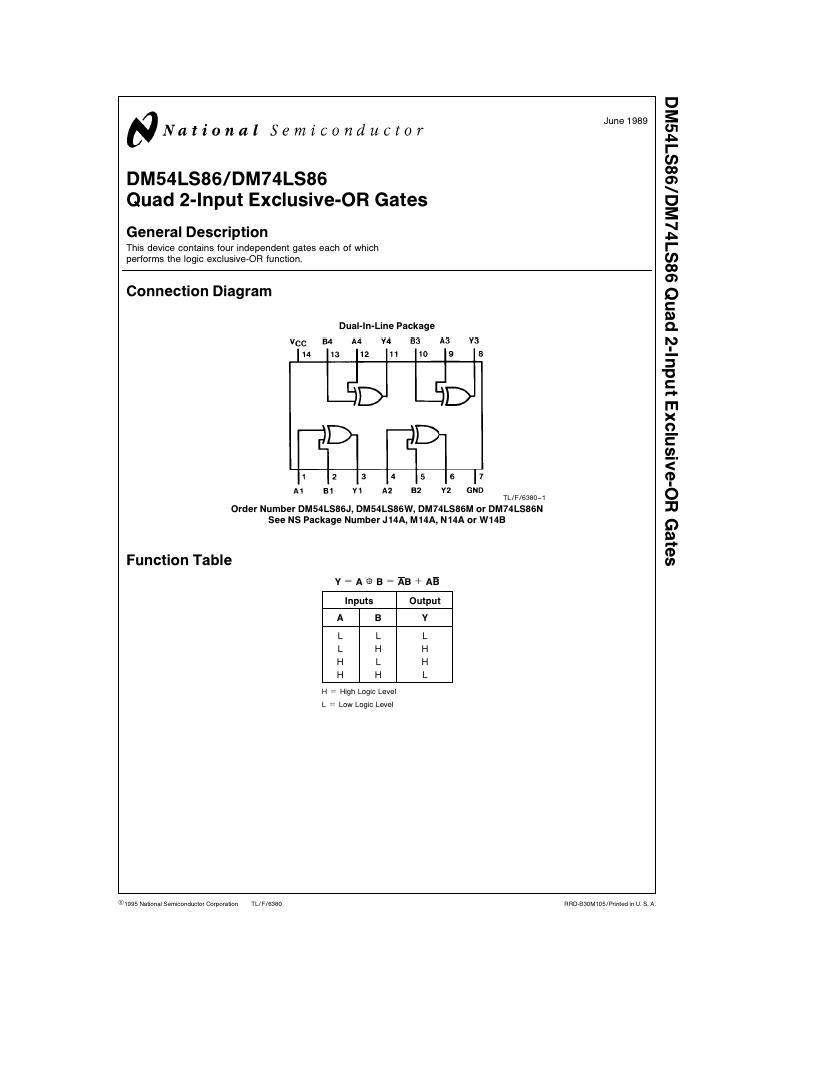
- Click on 'Next' button to Connect 'A' to Pin-1 of EX-OR Gate
- Click on 'Next' button to Connect 'B' to Pin-2 of EX-OR Gate
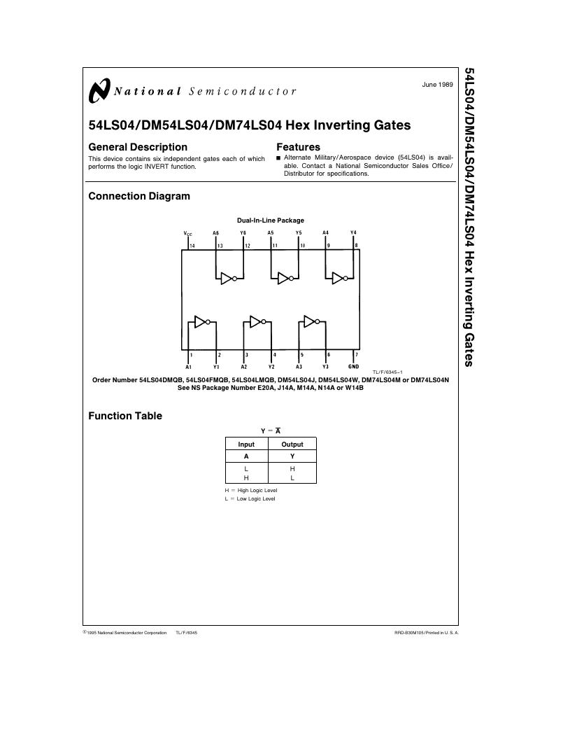
- Click on 'Next' button to Connect Pin-3 of Ex-OR to Pin-1 of NOT Gate
- Click on 'Next' button to Connect Pin-2 of NOT Gate to Output port as 'A=B'
- Click on 'Next' button to Connect 'A' to Pin-1 of AND Gate
- Click on 'Next' button to Connect 'B' to Pin-3 of NOT Gate
- Click on 'Next' button to Connect Pin-4 of NOT Gate to Pin-2 of AND Gate
- Click on 'Next' button to Connect Pin-3 of AND Gate to Output port as 'A>B'
- Click on 'Next' button to Connect 'B' to Pin-5 of AND Gate
- Click on 'Next' button to Connect 'A' to Pin-5 of NOT Gate
- Click on 'Next' button to Connect Pin-6 of NOT Gate to Pin-4 of AND Gate
- Click on 'Next' button to Connect Pin-6 of AND Gate to Output port as 'A<B'