Tutorial Start by tapping on Next button.
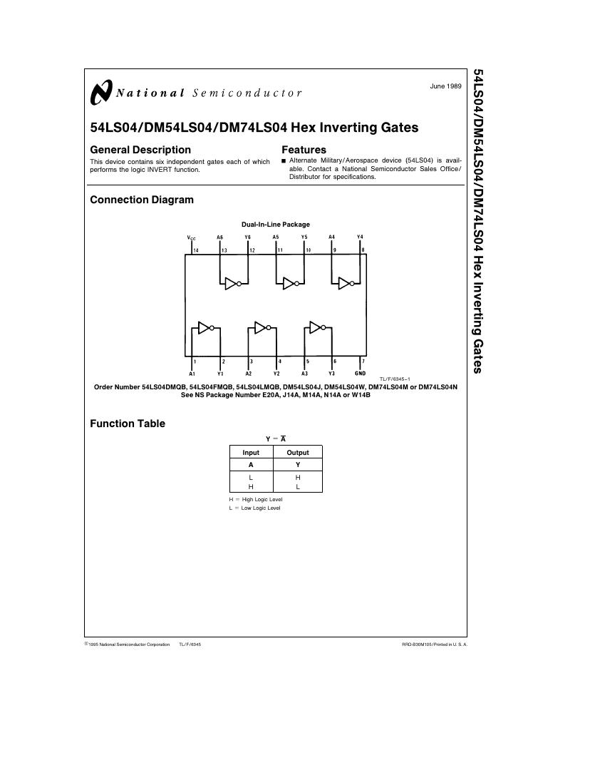
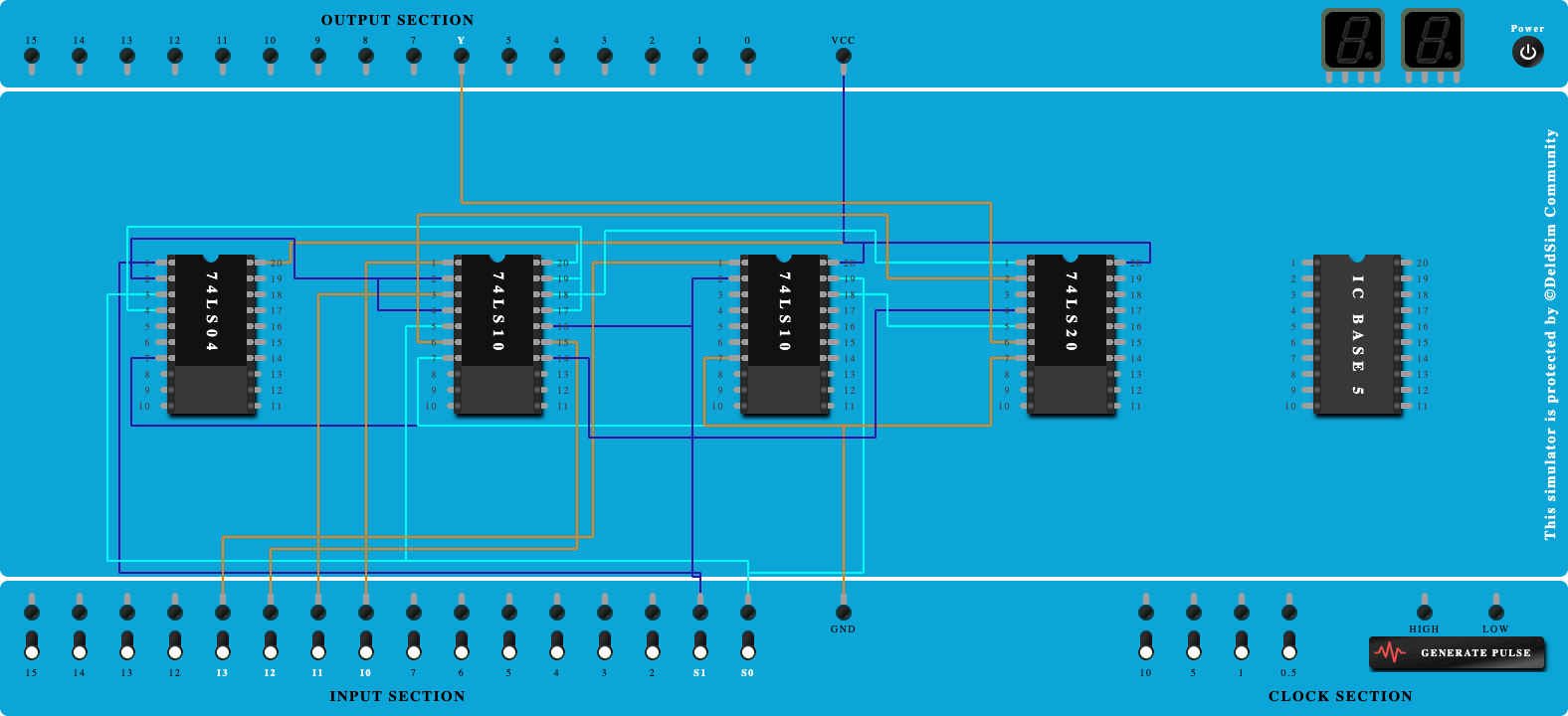
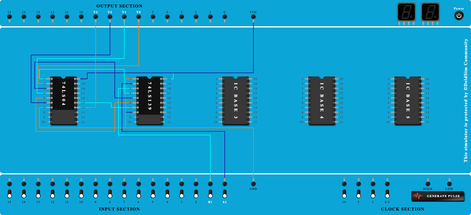
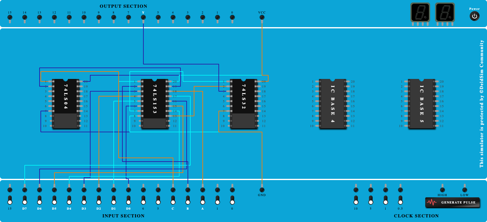
1. Click on 'Next' button to Add IC-74LS04 (NOT Gate) Click on 'Next' button to Add IC-74LS04 (NOT Gate)
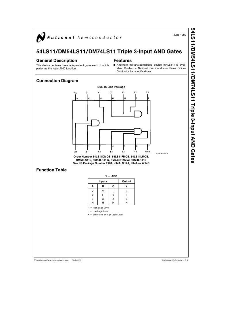
2. Click on 'Next' button to Add IC-74LS11 (3-Input AND Gate) Click on 'Next' button to Add IC-74LS11 (3-Input AND Gate)
3. Click on 'Next' button to Connect GND and VCC of all ICs Click on 'Next' button to Connect GND and VCC of all ICs
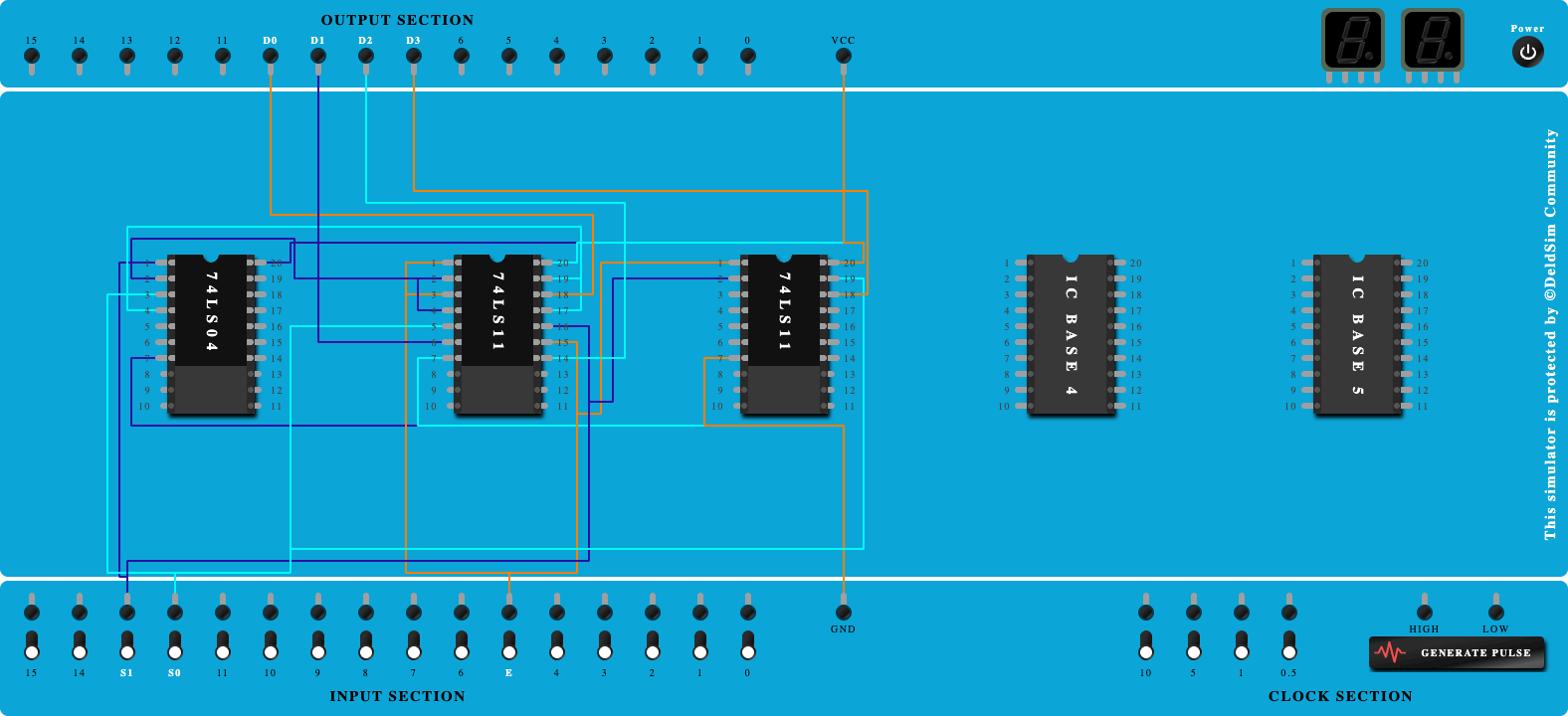
4. Click on 'Next' button to Connect Select line 'S1' to Pin-1 of NOT Gate Click on 'Next' button to Connect Select line 'S1' to Pin-1 of NOT Gate
5. Click on 'Next' button to Connect Select line 'S0' to Pin-3 of NOT Gate Click on 'Next' button to Connect Select line 'S0' to Pin-3 of NOT Gate
6. Click on 'Next' button to Connect Input 'E' to Pin-1 of AND Gate Click on 'Next' button to Connect Input 'E' to Pin-1 of AND Gate
7. Click on 'Next' button to Connect Inverse Output of 'S1' to Pin-2 of AND Gate Click on 'Next' button to Connect Inverse Output of 'S1' to Pin-2 of AND Gate
8. Click on 'Next' button to Connect Inverse Output of 'S0' to Pin-13 of AND Gate Click on 'Next' button to Connect Inverse Output of 'S0' to Pin-13 of AND Gate
9. Click on 'Next' button to Connect Input 'E' to Pin-3 of AND Gate Click on 'Next' button to Connect Input 'E' to Pin-3 of AND Gate
10. Click on 'Next' button to Connect Inverse Output of 'S1' to Pin-4 of AND Gate Click on 'Next' button to Connect Inverse Output of 'S1' to Pin-4 of AND Gate
11. Click on 'Next' button to Connect 'S0' to Pin-5 of AND Gate Click on 'Next' button to Connect 'S0' to Pin-5 of AND Gate
12. Click on 'Next' button to Connect Input 'E' to Pin-9 of AND Gate Click on 'Next' button to Connect Input 'E' to Pin-9 of AND Gate
13. Click on 'Next' button to Connect 'S1' to Pin-10 of AND Gate Click on 'Next' button to Connect 'S1' to Pin-10 of AND Gate
14. Click on 'Next' button to Connect Inverse Output of 'S0' to Pin-11 of AND Gate Click on 'Next' button to Connect Inverse Output of 'S0' to Pin-11 of AND Gate
15. Click on 'Next' button to Connect Input 'E' to Pin-1 of AND Gate-2 Click on 'Next' button to Connect Input 'E' to Pin-1 of AND Gate-2
16. Click on 'Next' button to Connect 'S1' to Pin-2 of AND Gate-2 Click on 'Next' button to Connect 'S1' to Pin-2 of AND Gate-2
17. Click on 'Next' button to Connect 'S0' to Pin-13 of AND Gate IC-2 Click on 'Next' button to Connect 'S0' to Pin-13 of AND Gate IC-2
18. Click on 'Next' button to Connect Output of AND GATE-1 to Output Port-10 Click on 'Next' button to Connect Output of AND GATE-1 to Output Port-10
19. Click on 'Next' button to Connect Output of AND GATE-2 to Output Port-9 Click on 'Next' button to Connect Output of AND GATE-2 to Output Port-9
20. Click on 'Next' button to Connect Output of AND GATE-3 to Output Port-8 Click on 'Next' button to Connect Output of AND GATE-3 to Output Port-8
21. Click on 'Next' button to Connect Output of AND GATE-4 to Output Port-7 Click on 'Next' button to Connect Output of AND GATE-4 to Output Port-7
Done You have completed the tutorial. Power on the circuit to test the behavior.