
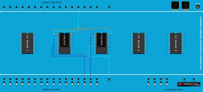
Integrated Circuits Used
Description
a is not then use it as input for or gate and b as it is
Procedure
- Add IC 74LS04 into ICBase-3 (74LS04).
- Connect Input-1 to Pin-1 (Input) of ICBase-3 (74LS04).
- Add IC 74LS32 into ICBase-2 (74LS32).
- Connect Output-3 to Pin-3 (Output) of ICBase-2 (74LS32).
- Connect Pin-1 (Input) of ICBase-2 (74LS32) to Pin-2 (Output) of ICBase-3 (74LS04).
- Connect Input-2 to Pin-2 (Input) of ICBase-2 (74LS32).
- Connect VCC Port to Pin-20 (VCC) of ICBase-3 (74LS04).
- Connect VCC Port to Pin-20 (VCC) of ICBase-2 (74LS32).
- Connect GND Port to Pin-7 (Ground) of ICBase-2 (74LS32).
- Connect GND Port to Pin-7 (Ground) of ICBase-3 (74LS04).