
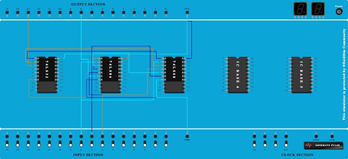
Integrated Circuits Used
Description
we are going to realise the full addaer thruth table we get the out put as per the circuit diagram that simplified using the boolean expression we connect the circuit using one 7432 OR gatr IC of 2 input OR gates and one ............!
Procedure
- Add IC 74LS32 into ICBase-1 (74LS32).
- Add IC 74LS86 into ICBase-2 (74LS86).
- Add IC 74LS08 into ICBase-3 (74LS08).
- Connect Pin-4 (Input) of ICBase-2 (74LS86) to Pin-3 (Output) of ICBase-2 (74LS86).
- Connect Input-8 to Pin-2 (Input) of ICBase-2 (74LS86).
- Connect Input-7 to Pin-1 (Input) of ICBase-2 (74LS86).
- Connect Input-6 to Pin-5 (Input) of ICBase-2 (74LS86).
- Connect Output-8 to Pin-6 (Output) of ICBase-2 (74LS86).
- Connect VCC Port to Pin-20 (VCC) of ICBase-2 (74LS86).
- Connect Pin-20 (VCC) of ICBase-3 (74LS08) to VCC Port.
- Connect VCC Port to Pin-20 (VCC) of ICBase-1 (74LS32).
- Connect GND Port to Pin-7 (Ground) of ICBase-1 (74LS32).
- Connect Pin-7 (Ground) of ICBase-2 (74LS86) to GND Port.
- Connect GND Port to Pin-7 (Ground) of ICBase-3 (74LS08).
- Connect Output-13 to Pin-3 (Output) of ICBase-1 (74LS32).
- Connect Input-7 to Pin-1 (Input) of ICBase-3 (74LS08).
- Connect Input-8 to Pin-2 (Input) of ICBase-3 (74LS08).
- Connect Pin-2 (Input) of ICBase-1 (74LS32) to Pin-3 (Output) of ICBase-3 (74LS08).
- Connect Pin-1 (Input) of ICBase-1 (74LS32) to Pin-6 (Output) of ICBase-3 (74LS08).
- Connect Pin-5 (Input) of ICBase-3 (74LS08) to Pin-3 (Output) of ICBase-2 (74LS86).
- Connect Input-6 to Pin-4 (Input) of ICBase-3 (74LS08).