
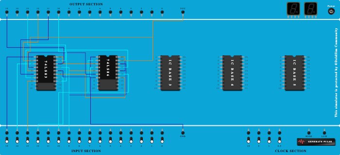
Integrated Circuits Used
Description
### BCD to Excess-3 Conversion Binary-Coded Decimal (BCD) represents decimal numbers using a four-bit format, while Excess-3 is a non-weighted code. The conversion process is simple and beneficial: 1. **Convert each BCD digit to decimal**: For example, BCD `0100` (4) and `0101` (5) represent 45. 2. **Add 3 to each digit**: So, 4 becomes 7, and 5 becomes 8. 3. **Convert the results to binary**: This gives 7 as `0111` and 8 as `1000`. 4. **Combine the results**: Hence, BCD `0100 0101` (45) converts to Excess-3 `0111 1000`. ### Excess-3 to BCD Conversion Converting Excess-3 back to BCD is just as straightforward: 1. **Convert Excess-3 to decimal**: For example, `0111` (7) and `1000` (8) represent 78. 2. **Subtract 3 from each digit**: Thus, 7 becomes 4, and 8 becomes 5. 3. **Convert to binary**: This results in 4 as `0100` and 5 as `0101`. 4. **Combine the results**: Therefore, Excess-3 `0111 1000` (78) becomes BCD `0100 0101`. These conversions simplify working with BCD and Excess-3 codes, enhancing efficiency!
Procedure
- Connect Input-15 to Pin-1 (Input) of ICBase-1 (74LS83).
- Connect Input-14 to Pin-3 (Input) of ICBase-1 (74LS83).
- Connect Input-13 to Pin-8 (Input) of ICBase-1 (74LS83).
- Add IC 74LS83 into ICBase-1 (74LS83).
- Add IC 74LS86 into ICBase-2 (74LS86).
- Connect Pin-1 (Input) of ICBase-2 (74LS86) to GND Port.
- Connect GND Port to Pin-4 (Input) of ICBase-2 (74LS86).
- Connect Pin-19 (Input) of ICBase-2 (74LS86) to VCC Port.
- Connect VCC Port to Pin-16 (Input) of ICBase-2 (74LS86).
- Connect Input-10 to Pin-2 (Input) of ICBase-2 (74LS86).
- Connect Input-9 to Pin-5 (Input) of ICBase-2 (74LS86).
- Connect Input-9 to Pin-18 (Input) of ICBase-2 (74LS86).
- Connect Pin-15 (Input) of ICBase-2 (74LS86) to Input-10.
- Connect Pin-3 (Output) of ICBase-2 (74LS86) to Pin-20 (Input) of ICBase-1 (74LS83).
- Connect Pin-4 (Input) of ICBase-1 (74LS83) to Pin-6 (Output) of ICBase-2 (74LS86).
- Connect Pin-17 (Output) of ICBase-2 (74LS86) to Pin-7 (Input) of ICBase-1 (74LS83).
- Connect Pin-15 (Input) of ICBase-1 (74LS83) to Pin-14 (Output) of ICBase-2 (74LS86).
- Connect Output-15 to Pin-18 (Output) of ICBase-1 (74LS83).
- Connect Output-13 to Pin-19 (Output) of ICBase-1 (74LS83).
- Connect Output-12 to Pin-2 (Output) of ICBase-1 (74LS83).
- Connect Output-11 to Pin-6 (Output) of ICBase-1 (74LS83).
- Connect Output-10 to Pin-13 (Output) of ICBase-1 (74LS83).
- Connect VCC Port to Pin-5 (VCC) of ICBase-1 (74LS83).
- Connect GND Port to Pin-16 (Ground) of ICBase-1 (74LS83).
- Connect Pin-17 (Input) of ICBase-1 (74LS83) to Input-9.
- Connect VCC Port to Pin-20 (VCC) of ICBase-2 (74LS86).
- Connect GND Port to Pin-7 (Ground) of ICBase-2 (74LS86).
- Connect Pin-14 (Input) of ICBase-1 (74LS83) to Input-12.
- Connect VCC Port to ICBase-2 (74LS86).
- Connect Input-8 to ICBase-2 (74LS86).
- Connect GND Port to ICBase-1 (74LS83).
- Connect Input-12 to ICBase-1 (74LS83).