
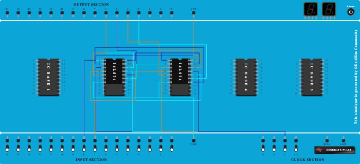
Integrated Circuits Used
Description
It performed well but here you have to first set all the CLR to 0 so all outputs are 0 and then set all CLR to 1 so that all outputs work normally
Procedure
- Connect Pin-3 (Input) of ICBase-2 (74LS74) to Clock port of 1Hz frequency.
- Connect Clock port of 1Hz frequency to Pin-17 (Input) of ICBase-2 (74LS74).
- Connect Clock port of 1Hz frequency to Pin-3 (Input) of ICBase-3 (74LS74).
- Connect Clock port of 1Hz frequency to Pin-17 (Input) of ICBase-3 (74LS74).
- Connect Input-8 to Pin-1 (Input) of ICBase-2 (74LS74).
- Connect Input-8 to Pin-19 (Input) of ICBase-2 (74LS74).
- Connect VCC Port to Pin-20 (VCC) of ICBase-2 (74LS74).
- Connect GND Port to Pin-7 (Ground) of ICBase-2 (74LS74).
- Connect Input-7 to Pin-4 (Input) of ICBase-2 (74LS74).
- Connect Input-7 to Pin-16 (Input) of ICBase-2 (74LS74).
- Connect GND Port to Pin-7 (Ground) of ICBase-3 (74LS74).
- Connect VCC Port to Pin-20 (VCC) of ICBase-3 (74LS74).
- Connect Input-8 to Pin-19 (Input) of ICBase-3 (74LS74).
- Connect Input-7 to Pin-16 (Input) of ICBase-3 (74LS74).
- Connect Input-7 to Pin-4 (Input) of ICBase-3 (74LS74).
- Connect Input-8 to Pin-1 (Input) of ICBase-3 (74LS74).
- Connect Pin-18 (Input) of ICBase-2 (74LS74) to Pin-5 (Output) of ICBase-2 (74LS74).
- Connect Output-6 to Pin-5 (Output) of ICBase-2 (74LS74).
- Connect Output-5 to Pin-15 (Output) of ICBase-2 (74LS74).
- Connect Pin-2 (Input) of ICBase-3 (74LS74) to Pin-15 (Output) of ICBase-2 (74LS74).
- Connect Pin-18 (Input) of ICBase-3 (74LS74) to Pin-5 (Output) of ICBase-3 (74LS74).
- Connect Pin-2 (Input) of ICBase-2 (74LS74) to Pin-14 (Output) of ICBase-3 (74LS74).
- Connect Output-3 to Pin-15 (Output) of ICBase-3 (74LS74).
- Connect Output-4 to Pin-5 (Output) of ICBase-3 (74LS74).
- Add IC 74LS74 into ICBase-3 (74LS74).
- Add IC 74LS74 into ICBase-2 (74LS74).