
Integrated Circuits Used
Description
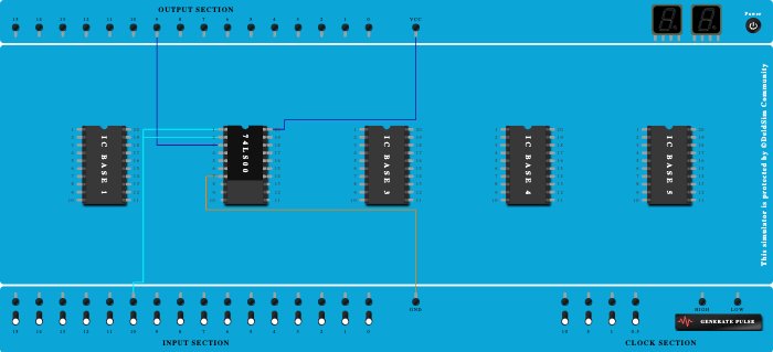
Implementation of NOT Gate using NAND Gate
Procedure
- Connect VCC Port to Pin-20 (VCC) of ICBase-2 (74LS00).
- Connect Pin-1 (Input) of ICBase-2 (74LS00) to Input-10.
- Connect GND Port to Pin-7 (Ground) of ICBase-2 (74LS00).
- Add IC 74LS00 into ICBase-2 (74LS00).
- Connect Pin-3 (Output) of ICBase-2 (74LS00) to Output-9.
- Connect Pin-2 (Input) of ICBase-2 (74LS00) to Input-10.