
Integrated Circuits Used
Description
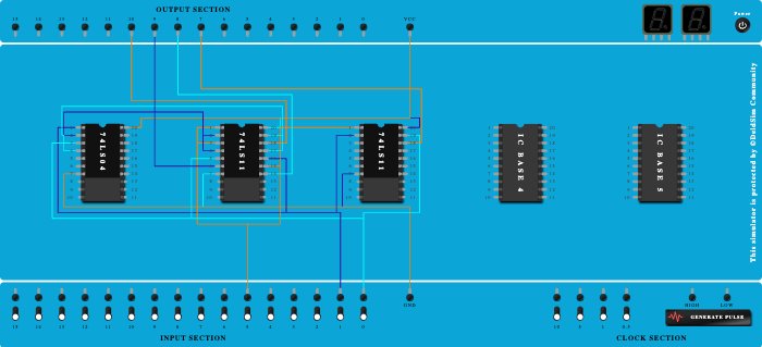
Using 2 triple 3 input AND gate , a NOT gate By considering S0 (input section 0) and S1 (input section 1) as selection lines and pin 5 of input section is considered as input and the pin 10,9,8,7 in output section are considered as outputs respectively Thereby , by connecting as per circuit diagram we'll get a 1X4 de-multiplexer
Procedure
- Add IC 74LS04 into ICBase-1 (74LS04).
- Add IC 74LS11 into ICBase-2 (74LS11).
- Add IC 74LS11 into ICBase-3 (74LS11).
- Connect GND Port to Pin-7 (Ground) of ICBase-3 (74LS11).
- Connect GND Port to Pin-7 (Ground) of ICBase-2 (74LS11).
- Connect GND Port to Pin-7 (Ground) of ICBase-1 (74LS04).
- Connect VCC Port to Pin-20 (VCC) of ICBase-3 (74LS11).
- Connect VCC Port to Pin-20 (VCC) of ICBase-2 (74LS11).
- Connect VCC Port to Pin-20 (VCC) of ICBase-1 (74LS04).
- Connect Input-1 to Pin-1 (Input) of ICBase-1 (74LS04).
- Connect Input-0 to Pin-3 (Input) of ICBase-1 (74LS04).
- Connect Input-5 to Pin-1 (Input) of ICBase-2 (74LS11).
- Connect Pin-2 (Output) of ICBase-1 (74LS04) to Pin-2 (Input) of ICBase-2 (74LS11).
- Connect Pin-4 (Output) of ICBase-1 (74LS04) to Pin-19 (Input) of ICBase-2 (74LS11).
- Connect Input-5 to Pin-3 (Input) of ICBase-2 (74LS11).
- Connect Pin-2 (Output) of ICBase-1 (74LS04) to Pin-4 (Input) of ICBase-2 (74LS11).
- Connect Input-0 to Pin-5 (Input) of ICBase-2 (74LS11).
- Connect Input-5 to Pin-15 (Input) of ICBase-2 (74LS11).
- Connect Input-1 to Pin-16 (Input) of ICBase-2 (74LS11).
- Connect Pin-4 (Output) of ICBase-1 (74LS04) to Pin-17 (Input) of ICBase-2 (74LS11).
- Connect Input-5 to Pin-1 (Input) of ICBase-3 (74LS11).
- Connect Input-1 to Pin-2 (Input) of ICBase-3 (74LS11).
- Connect Input-0 to Pin-19 (Input) of ICBase-3 (74LS11).
- Connect Output-10 to Pin-18 (Output) of ICBase-2 (74LS11).
- Connect Output-9 to Pin-6 (Output) of ICBase-2 (74LS11).
- Connect Output-8 to Pin-14 (Output) of ICBase-2 (74LS11).
- Connect Output-7 to Pin-18 (Output) of ICBase-3 (74LS11).