
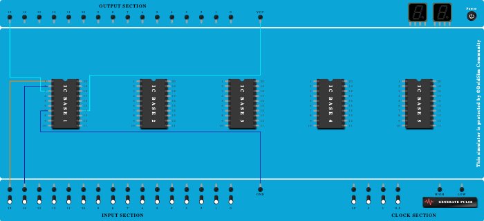
Description
Digital logic design
Procedure
- Connect GND Port to Pin-7 (Input & Output) of ICBase-1.
- Connect VCC Port to Pin-14 (Input & Output) of ICBase-1.
- Connect Pin-1 (Input & Output) of ICBase-1 to Input-15.
- Connect Pin-2 (Input & Output) of ICBase-1 to Input-14.
- Connect Output-15 to Pin-3 (Input & Output) of ICBase-1.