
Integrated Circuits Used
Procedure
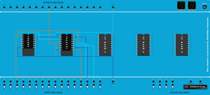
- Add IC 74LS151 into ICBase-2 (74LS151).
- Add IC 74LS04 into ICBase-1 (74LS04).
- Connect GND Port to Pin-8 (Ground) of ICBase-2 (74LS151).
- Connect VCC Port to Pin-20 (VCC) of ICBase-2 (74LS151).
- Connect GND Port to Pin-4 (Input) of ICBase-2 (74LS151).
- Connect VCC Port to Pin-1 (Input) of ICBase-2 (74LS151).
- Connect VCC Port to Pin-18 (Input) of ICBase-2 (74LS151).
- Connect GND Port to Pin-7 (Input) of ICBase-2 (74LS151).
- Connect GND Port to Pin-7 (Ground) of ICBase-1 (74LS04).
- Connect VCC Port to Pin-20 (VCC) of ICBase-1 (74LS04).
- Connect Pin-13 (Input) of ICBase-2 (74LS151) to Input-3.
- Connect Pin-14 (Input) of ICBase-2 (74LS151) to Input-2.
- Connect Pin-15 (Input) of ICBase-2 (74LS151) to Input-1.
- Connect Pin-1 (Input) of ICBase-1 (74LS04) to Input-0.
- Connect Pin-2 (Input) of ICBase-2 (74LS151) to Pin-2 (Output) of ICBase-1 (74LS04).
- Connect Pin-3 (Input) of ICBase-2 (74LS151) to Pin-2 (Output) of ICBase-1 (74LS04).
- Connect Pin-17 (Input) of ICBase-2 (74LS151) to Pin-2 (Output) of ICBase-1 (74LS04).
- Connect Pin-19 (Input) of ICBase-2 (74LS151) to Input-0.
- Connect Pin-16 (Input) of ICBase-2 (74LS151) to Input-0.
- Connect Output-8 to Pin-5 (Output) of ICBase-2 (74LS151).