Learning Objectives
- To understand the behavior and demonstrate the operation of Triple 3-Input AND Gate
- To apply knowledge of the fundamental gates to create truth tables.
- To develop digital circuit building and troubleshooting skills.
- To understand key elements of TTL logic specification or datasheets.
Integrated Circuits Used
Circuit Tutorials
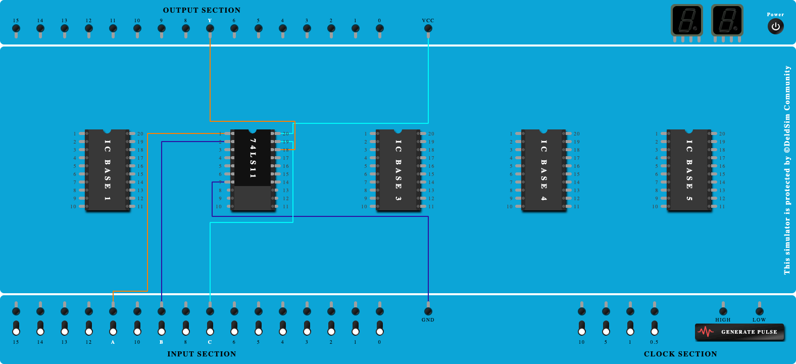
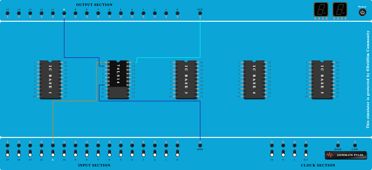
Procedure
- Place the IC on IC Trainer Kit.
- Connect VCC and ground to respective pins of IC Trainer Kit.
- Implement the circuit as shown in the circuit diagram.
- Connect the inputs to the input switches provided in the IC Trainer Kit.
- Connect the outputs to the switches of O/P LEDs
- Apply various combinations of inputs according to the truth table and observe the condition of LEDs.
- Note down the corresponding output readings for various combinations of inputs.
- Power Off Trainer Kit, disconnect all the wire connections and remove IC's from IC-Base.
Theory
AND GATE - It is a digital circuit that has two or more inputs and produces an output, which is the logical AND of all those inputs. It is optional to represent the Logical AND with the symbol ‘.’
Logic AND Gates are available using digital circuits to produce the desired logical function and is given a symbol whose shape represents the logical operation of the AND gate. Because the Boolean expression for the logic AND function is defined as (.), which is a binary operation, AND gates can be cascaded together to form any number of individual inputs. However, commercial available AND gate IC’s are only available in standard 2, 3, or 4-input packages. If additional inputs are required, then standard AND gates will need to be cascaded together to obtain the required output value.
Boolean Expression Y = A.B.C
"If A and B and C are true, then Y is true"

This AND gate produces an output Y, which is the logical AND of inputs A, B, C.
Block Diagram

Precautions
- Make the connections according to the IC pin diagram.
- The connections should be tight on trainer kit.
- The Vcc and ground should be applied carefully at the specified pin only.
Conclusion
Related Study Materials
8-Input NAND Gate

To study and verify the truth table of 8-Input NAND Gate
Quad 2-input NAND Gates with Open-Collector Outputs using 74LS38
To study and verify the truth table of Quad 2-input NAND Gates with Open-Collector Outputs using 74LS38.

Implementation of AND Gate using NAND gate
To study and verify the Implementation of AND Gate using NAND gate.
Hex Inverters with Open-Collector Outputs using 74LS14
To study and verify the truth table of Hex Inverters with Open-Collector Outputs using 74LS14.

Hex Inverters with Open-Collector Outputs using 74LS05
To study and verify the truth table of Hex Inverters with Open-Collector Outputs using 74LS05.